


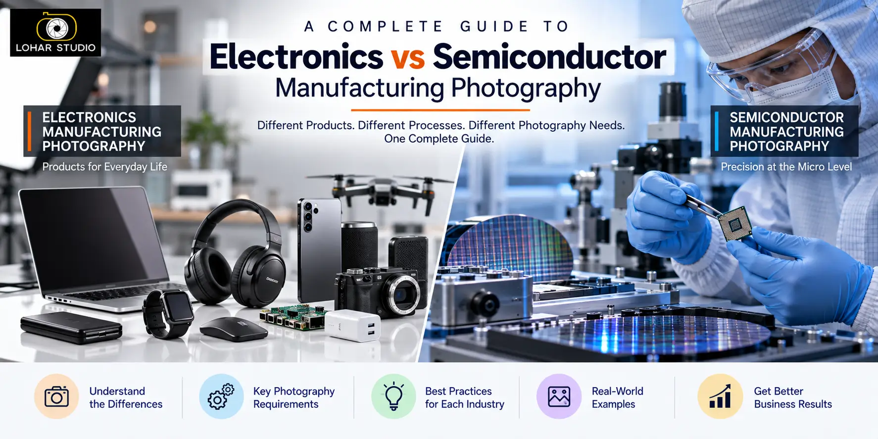
Electronics manufacturing photography documents PCB assembly, SMT lines, and finished-device production on an open or lightly controlled factory floor. Semiconductor manufacturing photography documents wafer fabrication inside an ISO-classified cleanroom, where ESD protocols, gowning, and equipment restrictions change almost everything about how the shoot is planned and executed. The two are related but require different gear, different access clearances, and different photographic techniques.
If you manufacture PCBs, assemble consumer devices, or run a chip fab in Delhi NCR and you're trying to figure out what kind of photography your facility actually needs — this guide breaks it down properly.
Why This Distinction Matters for Your Business
Most Indian manufacturers use "electronics photography" as a catch-all term. But an investor deck for a semiconductor fab and a product catalogue shoot for a PCB assembly unit are not the same job. Get this wrong when briefing a photographer and you'll end up with a shoot that can't legally happen (unauthorized cleanroom entry), or one that under-delivers (generic factory shots that don't show what actually makes a fab impressive: precision, sterility, scale).
At Lohar Studio, we've photographed both — PCB assembly lines, SMT placement machines, and cleanroom-adjacent semiconductor facility exteriors and gowning areas across Delhi NCR's industrial belt (Noida, Greater Noida, Manesar are seeing real semiconductor investment right now). Here's what 16+ years on factory floors has taught us about where these two disciplines diverge.
What Is Electronics Manufacturing Photography?
Electronics manufacturing photography covers the visual documentation of facilities that assemble finished electronic products or components — think PCB assembly plants, SMT (surface-mount technology) lines, consumer electronics assembly (appliances, chargers, gadgets), and electrical component manufacturing.
Typical subjects:
- SMT pick-and-place machines placing components on circuit boards
- Wave soldering and reflow oven lines
- Manual/semi-automated assembly stations
- Quality inspection and testing benches
- Finished product packaging lines
- Workers in standard ESD coats (not full cleanroom gowning)
Access level: Most electronics assembly floors are ISO Class 7–8 at most (or no formal cleanroom classification at all), meaning a photographer can usually work with standard factory safety gear — ESD wrist straps, basic PPE, and sometimes an ESD smock over regular clothing.
Electronics Photography for Amazon
In the competitive world of e-commerce, high-quality electronics product images play a crucial role in attracting customers and in...
Explore Electronics Photography for AmazonWhat Is Semiconductor Manufacturing Photography?
Semiconductor manufacturing photography documents the far more controlled environment of wafer fabrication — the "fab" — where silicon wafers go through deposition, photolithography, etching, and doping to become integrated circuits.
Typical subjects:
- Wafer handling and pick-and-place at the die level
- Photolithography and etching equipment (usually shown from outside due to access restrictions)
- Gowning/gowning-room entry sequences
- Cleanroom corridors and equipment bays
- Wafer inspection stations
- Fully gowned technicians (bunny suits, hoods, face masks, gloves)
Access level: This is the critical difference. Most wafer fabrication happens in semiconductor cleanrooms designed to maintain extremely low levels of airborne particles, temperature fluctuations, humidity variations, static, and molecular contamination, typically ISO 14644-1 Class 4–6 for wafer fabrication, with less particle-sensitive steps like assembly, packaging, or testing sometimes using ISO Class 7 or 8. Cameras, lenses, and even a photographer's own clothing and skin cells are contamination risks. This isn't a "bring your gear and shoot" environment.
Electronics vs Semiconductor Manufacturing Photography: Side-by-Side
| Factor | Electronics Manufacturing Photography | Semiconductor Manufacturing Photography |
|---|---|---|
| Environment | Open factory floor, standard ESD zones | ISO-classified cleanroom (often Class 4–8) |
| Gowning required | Basic ESD coat, sometimes optional | Full bunny suit, hood, gloves, mask, booties |
| Camera/gear restrictions | Minimal — standard DSLR/mirrorless fine | Camera and lenses must be cleanroom-cleaned; some fabs restrict external equipment entirely |
| ESD risk | Moderate — managed with wrist straps | Severe — a single discharge can destroy a wafer die |
| Subject scale | Human-scale (boards, components, machines) | Micro-scale (wafers, dies) shot via macro or supplied imagery |
| Typical access approval | Facility manager sign-off | Multi-level clearance, NDA, sometimes fab engineering approval |
| Common use case | E-commerce catalogues, investor decks, export brochures | Investor decks, government/PLI scheme documentation, corporate reports |
| Shoot duration | Standard half-day to full-day | Often shorter, tightly scheduled around production windows |
The Cleanroom Problem: Why You Can't Just "Bring a Camera"
This is the part most manufacturers don't anticipate. In a semiconductor fab, a single contaminating particle smaller than a wavelength of visible light can destroy a transistor gate, short-circuit a memory cell, or render an entire wafer useless — which is exactly why microelectronic and semiconductor cleanrooms range from Class 100 to Class 100,000 depending on the processes taking place within the facility.
Electronics Photography for Flipkart
Looking for Electronics Product Photography for Flipkart? At Lohar Studio, we specialize in capturing high-quality, professional e...
Explore Electronics Photography for FlipkartPhotographers working near or inside these spaces need to understand a few operational realities:
- ESD is not optional. Cleanroom furniture is often equipped with metal discharge chains that drag along the perforated floor to keep electrical charge build-up to a minimum, and workers wear wrist grounding straps connected to ground. A photographer's camera body, tripod, and even lens caps can carry static charge.
- Airflow is engineered, not incidental. Air is blown from the ceiling down to the floor in a constant, uniform stream — Vertical Laminar Flow — passing through perforated floor holes and HEPA filters before recirculating. Stepping into a wafer bay with unauthorized equipment can disrupt this.
- Most real production shots are impossible. Because of contamination and IP risk, many semiconductor companies don't allow photography of live wafer processing at all. Realistic deliverables usually include: facility exteriors, gowning room sequences, corridors, control rooms, R&D labs, and staged/approved equipment shots — not the wafer floor itself.
For electronics assembly plants, none of this applies at the same intensity — which is exactly why treating both shoots the same way produces disappointing results either way: over-preparing (and over-charging) for a standard SMT line, or under-preparing for a fab.
What This Means for Your Photography Brief
If you're commissioning a shoot, be specific about which category you fall into:
- PCB assembly / SMT / consumer electronics manufacturer → standard industrial photography brief works. Focus on production flow, quality control, and finished product context.
- Semiconductor fab / wafer processing facility → brief your photographer on cleanroom protocol before the shoot. Confirm what's actually shootable (usually not the wafer bay itself), gowning requirements, and equipment restrictions in advance.
- Hybrid facility (component + assembly) → plan two distinct shot lists, since lighting, access, and gear needs differ by zone.
This is also where a lot of Delhi NCR's growing semiconductor and electronics ecosystem gets it wrong in marketing materials — using generic stock-style factory images that don't reflect the actual precision of what's happening on-site, whether that's an SMT line or a fab.
10 FAQs: Electronics vs Semiconductor Manufacturing Photography
1. What's the main difference between electronics and semiconductor manufacturing photography?
.webp)
Electronics Photography in Delhi
Lohar Studio offers electronics product photography in Delhi for e-commerce sellers, D2C gadget brands, and electronics manufactur...
Explore Electronics Photography in DelhiElectronics manufacturing photography documents PCB assembly and device production on a standard factory floor. Semiconductor photography documents wafer fabrication inside an ISO-classified cleanroom with strict ESD and contamination controls.
2. Can a regular industrial photographer shoot inside a semiconductor cleanroom?
Only with proper cleanroom protocol — gowning, cleaned/approved equipment, and facility clearance. Not every industrial photographer has this experience or the fab's sign-off to enter.
3. Do semiconductor fabs allow photography of the actual wafer processing line?
Rarely. Most fabs restrict photography of live wafer processing due to IP and contamination risk. Approved shoots typically cover exteriors, gowning areas, corridors, control rooms, and R&D spaces.
4. What camera equipment is needed for semiconductor cleanroom photography?
Equipment must be cleanroom-compatible — cleaned, minimal, and sometimes restricted to what the facility itself permits. Standard DSLR bodies and lenses often can't enter Class 4–6 areas without specific clearance.
5. Is ESD a concern in electronics manufacturing photography too?
Yes, but at a lower intensity. Standard ESD coats and wrist straps are usually sufficient for PCB/SMT floors, compared to full gowning required in semiconductor fabs.
Industrial Photography in Delhi
Thousands of manufacturing companies across Delhi NCR still use dark, blurry mobile phone images on their websites, brochures, and...
Explore Industrial Photography in Delhi6. What ISO cleanroom class do semiconductor fabs typically use?
Most wafer fabrication occurs in ISO 14644-1 Class 4–6 cleanrooms, while less particle-sensitive steps like assembly, packaging, or testing may use ISO Class 7 or 8.
7. What can realistically be photographed at a semiconductor facility for a company profile or investor deck?
Facility exteriors, reception/lobby areas, gowning sequences, control rooms, R&D labs, staged equipment shots (with approval), and corporate/team photography — rather than live wafer processing.
8. How long does a semiconductor facility shoot typically take compared to an electronics plant shoot?
Semiconductor shoots are often shorter and more tightly scheduled around production windows and clearance logistics, while electronics assembly shoots can run a full day with more flexibility.
9. Why does Delhi NCR matter for electronics and semiconductor manufacturing photography right now?
Delhi NCR's industrial belt — Noida, Greater Noida, Manesar, Bawana — is seeing rising investment in electronics and semiconductor manufacturing under India's PLI scheme, increasing demand for professional documentation for investor and compliance purposes.
10. Should I hire different photographers for electronics vs semiconductor manufacturing photography?
Not necessarily different photographers, but definitely a photographer with demonstrated experience in both cleanroom protocol and standard industrial shoots — the skill sets don't fully overlap, so ask about specific past access to controlled environments.
If you're looking to enhance your brand’s presence on leading e-commerce platforms like Amazon, Flipkart, Myntra, Meesho, TataCliQ, Snapdeal, and Ajio, Lohar Studio is your go-to destination. Our team specializes in delivering high-quality images for fashion items, footwear, automotive products, medical photography, business headshots, and corporate shoots. We serve Delhi, Noida, Gurgaon, Faridabad, and Ghaziabad, offering professional results that boost conversions and elevate your brand’s image. Get in touch today at +91 9312070458 or visit us at A1/58, 1st Floor, Sector 6 Rd, Pocket 1, Sector 6A, Rohini, Delhi, 110085, to schedule your next shoot!

Written from hands-on experience shooting for 4000+ brands - practical, field-tested photography advice, not just theory.